
Table of Contents
Silicon isn’t the only semiconductive material used to make solar cells.
But it is the most commonly used by far.
Over 90% of solar panels sold today rely on silicon wafer-based cells.
Silicon is also used in virtually every modern electronic device, including the one you’re reading this on…
Unless you printed it out.
Silicon Valley got the name for a reason — and less refined forms of silicon are also used to manufacture concrete, glass, and silicone rubber.
Silicon is found everywhere — it’s the second most abundant element on Earth.
But, the pure silicon crystals required to make solar-grade wafers are very different from sand on the beach.
Read on to learn more about silicon wafers for solar cells.
What Is a Wafer-Based Solar Cell?
Solar cells are an essential part of systems that convert sunlight into electricity using the photovoltaic effect.
Wafer-based solar cells are the most commonly used photovoltaic (PV) cells by far.
Most PV modules — like solar panels and shingles — contain at least several and up to hundreds of wafer-based crystalline silicon solar cells.
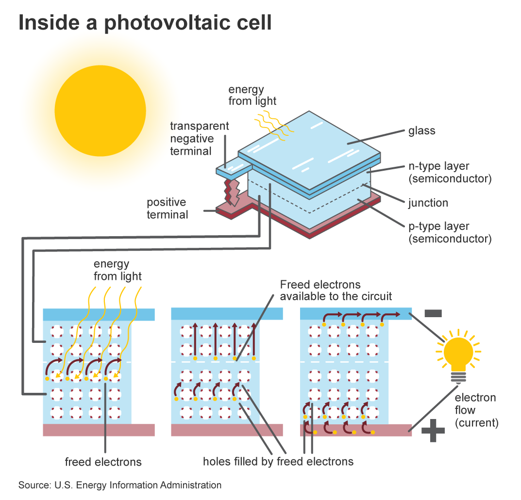
(Source: EIA)
How Does a Wafer-Based Solar Cell Function?
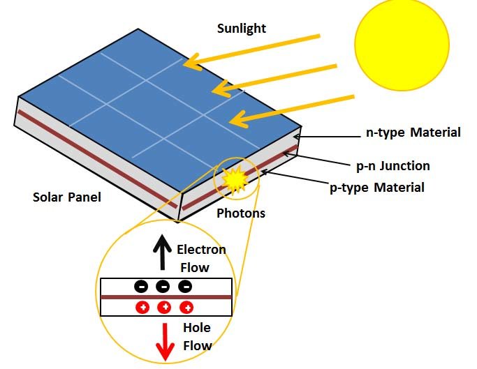
A wafer-based solar cell is a unique type of non-mechanical semiconductor that uses a p-n junction to produce the photovoltaic effect — transforming photons from sunlight into direct current electricity.
Semiconductors are an essential component of almost all modern electronic devices and appliances and fall under two classifications.
Intrinsic Semiconductors
Intrinsic semiconductors — like silicon (Si) and germanium (Ge) — are metalloid chemical elements not found in pure form in the Earth’s crust.
Both elements require significant processing to be extracted from commonly found materials like sand and quartz in a process called reduction.
Germanium is sometimes combined with silicon in highly specialized — and expensive — photovoltaic applications.
However, purified crystalline silicon is the photovoltaic semiconductor material used in around 95% of solar panels.
For the remainder of this article, we’ll focus on how sand becomes the silicon solar cells powering the clean, renewable energy revolution.
Extrinsic Semiconductors
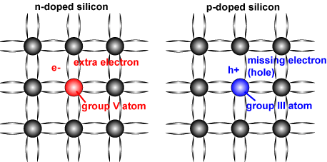
Extrinsic semiconductors are made by intentionally introducing chemical impurities that improve the electrical properties of a purified material like silicon.
Adding tiny amounts of chemicals like boron and phosphorous to purified silicon is called doping.
Purified silicon is used to make extrinsic semiconductors — like those used in solar cells.
However, the conductivity of intrinsic semiconductors is too low and sensitivity to temperature too high to perform adequately in modern electronic devices.
Only by adding dopants to intrinsic semiconductive materials can we manufacture the extrinsic semiconductors found in virtually every electrical device, from transistors and diodes to microchips and solar panels.
(Source: US Dept. of Energy)
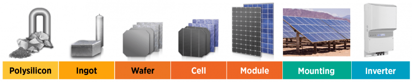
How Are Silicon Wafers Made?
Silicon wafers have multiple applications — not just solar panels — and manufacturing silicon wafers is a multi-step process.
Here, we’ll focus on the process behind manufacturing silicon wafers for use in high-efficiency monocrystalline silicon solar panels.
Mining Sand and Quartz
When you hear the word sand, you probably think of the beach.
But sand is also one of the most mined materials on Earth, with 50 billion tons extracted each year.
Sand itself is not a mineral but rather a sediment composed of a wide variety of materials.
Depending on where sand is mined from, it may contain:
- Quartz and quartzite
- Feldspar
- Calcium carbonate
- Glass
The essential mineral for making silicon wafers is quartz.
There are many different types of sand around the world, and the supply may seem endless.
But it’s not.
One reason for the “sand shortage” is that desert sand is rarely used to make cement or silicon.
Sand eroded by water — like beach or river sand — is a far more valuable commodity, and we consume it at a much faster rate than it’s replenished by nature.
Just like fossil fuels.
However, the negative environmental impact of mining sand for use in solar panels is minuscule compared to the benefits of switching to a renewable energy source to produce electricity in place of gas, oil, and coal.
The sand used to produce semiconductor-grade silicon is called silica sand or quartz sand.
Silica sand is found all over the world, with China and the United States being the leading producers and consumers of mined quartz sand.
Sand or gravel must contain at least 95% silicon dioxide and less than 0.6% iron oxide to be classified as silica (SiO2).
For electrical applications that require the purest silicon, quartz rock is used instead of sand.
Most of the quartz rock for semiconductors like microchips comes from just four countries. In order of production, they are:
- United States
- South Korea
- Germany
- Japan
The world’s purest quartz is mined near Spruce Pine, North Carolina.
One industry expert told the BBC, “It does boggle the mind a bit to consider that inside nearly every cell phone and computer chip you’ll find quartz from Spruce Pine.”
Silicon solar wafers can be made from either quartz rock or silica sand, although quartz rock is a considerably more expensive material.
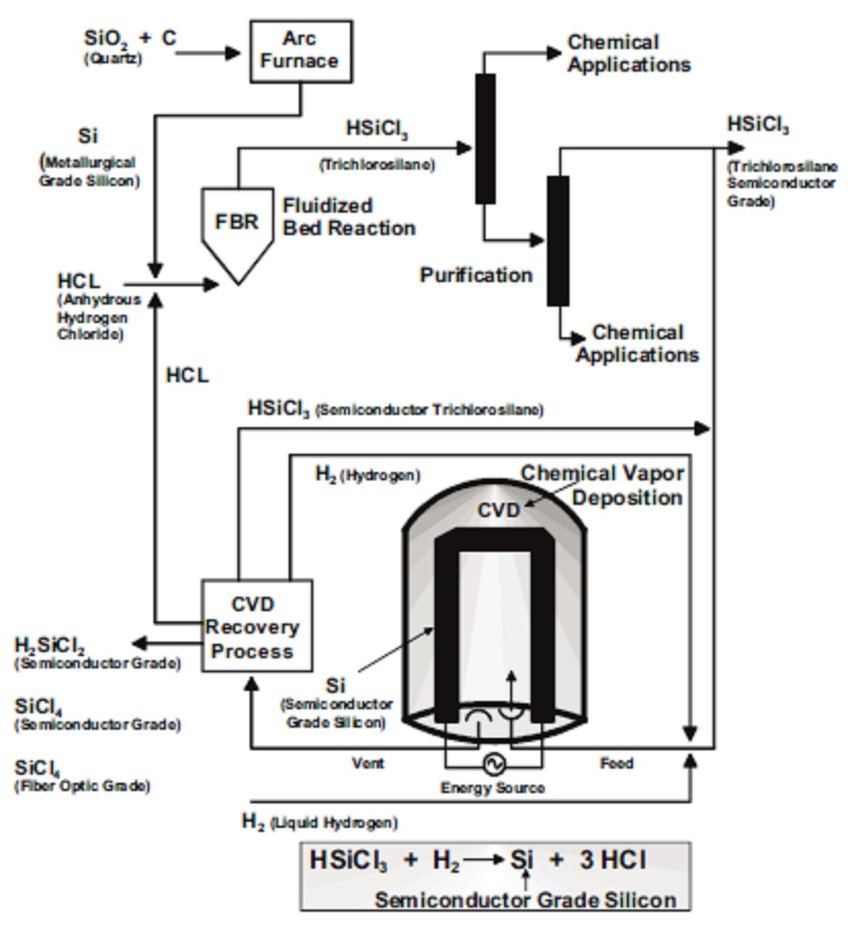
Turning Silica Sand and Quartz Into Silicon
Once extracted, silica sand or quartz must undergo a smelting process to produce metallurgical silicon.
The raw material is combined with coke — not the soft drink, but a type of coal — and woodchips, which produce carbon when heated.
The mixture is fired in massive industrial furnaces that reach temperatures of 3,600°F (2000°C) or higher.
A significant amount of electricity is also required — about 10-12 MWh per ton of silicon.
The carbothermal reduction process (smelting) results in metallurgical-grade silicon (MG-Si or MGS), which is sufficiently pure for many industrial applications.
Purification
For use as a semiconductor in most applications, silicon must be 99% pure.
For high-end computer chips and microprocessors, the purity of silicon required is up to 99.99999999999%.
Solar-grade silicon can be marginally less pure at 7N to 10N — that’s 99% + 7 to 10 Ninths.
Extensive processing of metallurgical-grade silicon is required to achieve purity at such levels.
The most widely used purification method for solar-grade polysilicon is known as the Siemens Process.
(Source: ResearchGate)
The Siemens Process
Multiple attempts have been made to develop less costly and more efficient methods of producing solar-grade polysilicon, but the Siemens Process remains the most widely used.
The process was developed in the 1950s and is still used to produce an estimated 90% of the total volume of polysilicon used to make solar wafers and semiconductors for electronics.
The primary raw material (feedstock) for the Siemens Process is metallurgical-grade silicon (MG-Si).
MG-SI is ~98.5% pure.
The Siemens Process purifies MG-Si still further to produce solar-grade polysilicon.
Here are the basic steps.
- Metallurgical-grade silicon is crushed into a fine powder.
- The MG-Si crystals are fluidized with hydrochloric acid (HCI) in a distillation column to produce liquid trichlorosilane (SiHCl3 or TCS).
- In a steel bell jar reactor, trichlorosilane is deposited onto pure silicon filaments that are electrically heated up to 2,102°F (1,150 °C). This is known as chemical vapor deposition (CVD).
- The end product of CVD is purified polysilicon rods with a diameter of 15 to 20cm grown in the reactor. Byproducts like silicon tetrachloride (SiCl4, or STC) are recycled through hydrochlorination and fed back into the beginning of the process.
(Source: ReseachGate)
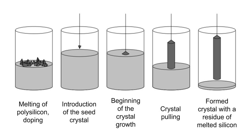
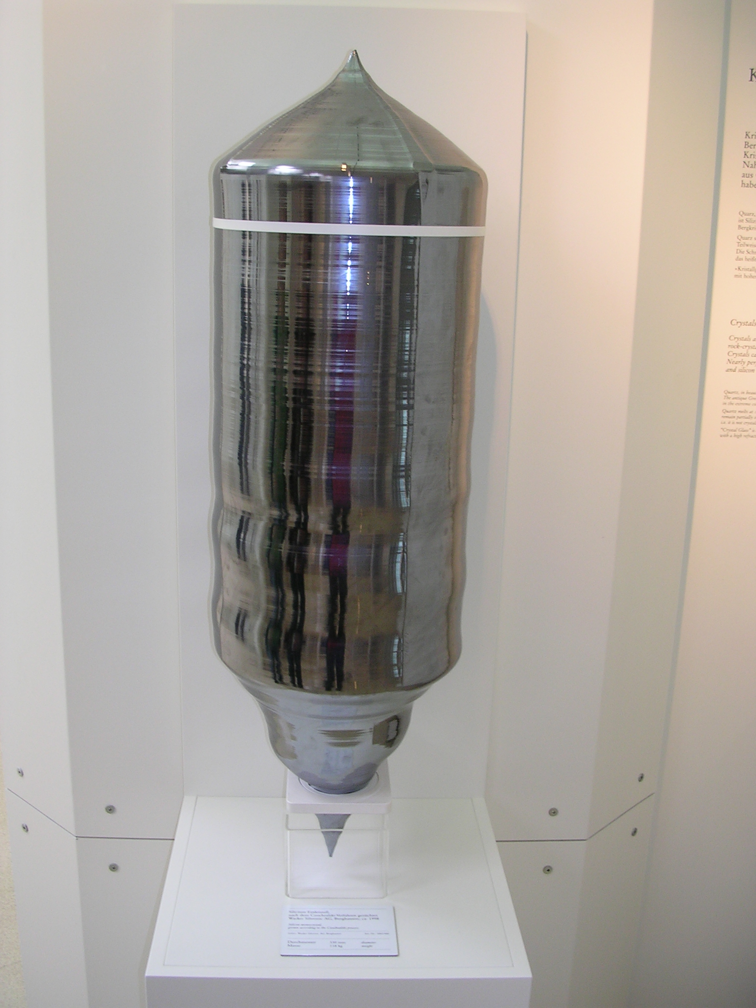
The Czochralski Method — From Polysilicon Rods to Crystalline Silicon Ingots
Following completion of the Siemens process, the long, purified polysilicon rods are broken down into uniform chunks, packaged, and ready for further processing.
There are several methods for producing pure monocrystalline silicon ingots, including the Bridgman
and Float Zone techniques.
However, the vast majority of solar-grade silicon wafers are produced using the Czochralski method.
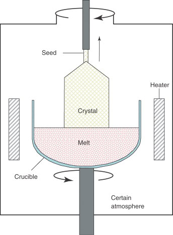
The Czochralski technique grows pure monocrystalline ingots by melting chunks of polysilicon rods as feedstock in a cylindrical quartz crucible fused from high purity Silica (SiO2).
Quartz crucibles are capable of withstanding extreme heat of up to ~2640°F (1450°C).
The polysilicon feedstock is melted in the crucible at a temperature of around 2600°F (1420°C).
Doping
Once the feedstock is melted, the dopants boron or phosphorous are added in minute quantities.
(Source: PV Education)
Adding dopants changes the electrical properties of the silicon — an essential step for creating P-type and N-type semiconductor materials that solar cells require.
(Source: Research Gate)
Doping with boron creates N-type (negative) silicon. Phosphorous doping produces P-type (positive) silicon.
A P-N junction produces the photovoltaic effect and converts the photons from sunlight into DC electricity.
(Source: ScienceDirect)
Seeding the Silicon
A single pure silicon seed crystal is dipped into the molten silicon feedstock.
Seed crystals for solar-grade wafers are, at most, a few millimeters in diameter.
Once the seed crystal is inserted, a melt meniscus is formed.
The seed crystal is then slowly withdrawn.
(Source: ResearchGate)
Pulling Silicon
“Pulling” the silicon from the crucible is one of the most critical steps of the Czochralski process.
How the silicon is pulled determines many aspects of the end product, including the size of the ingot and wafers.
The following aspects of pulling silicon are precisely controlled:
- Individual rotation rate of both crucible and seed
- Heat application
- Pulling velocity
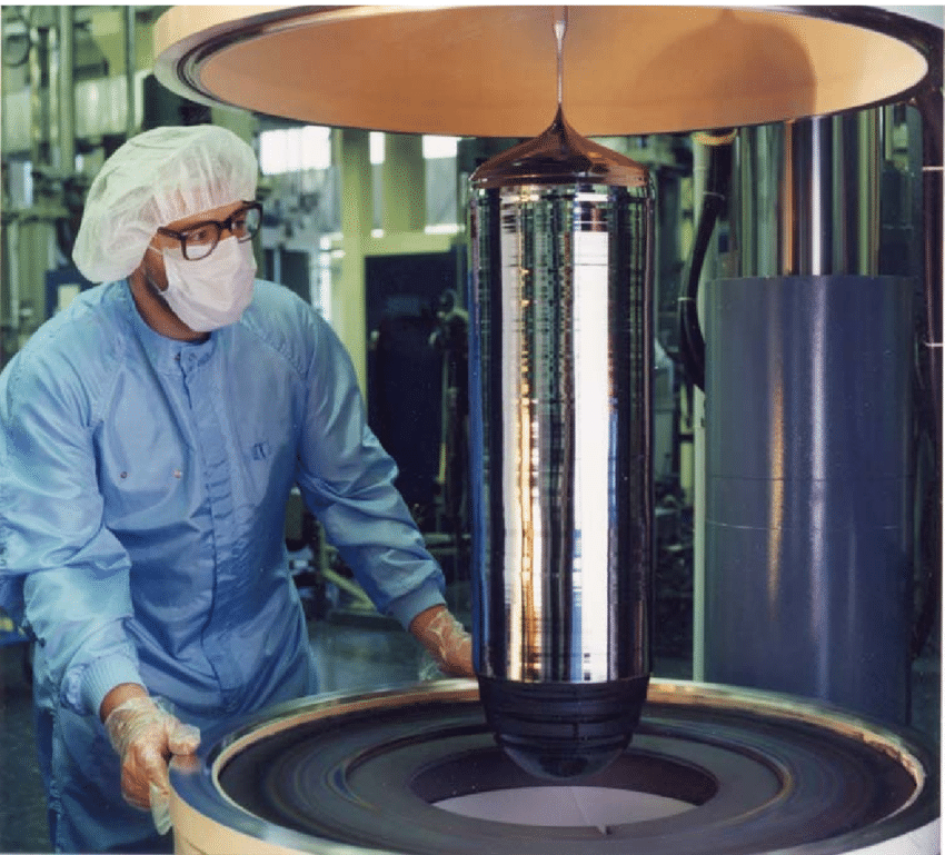
Once the pulling process is complete, the end product is a monocrystalline silicon ingot — ready to be turned into wafers for photovoltaic cells.
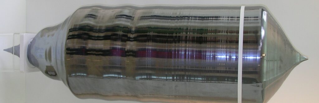
(Source: Wikimedia/Creative Commons)
From Monocrystalline Silicon Ingot to Solar Grade-Wafers
Once the growing stage is complete, the Czochralski (CZ) silicon ingot is ready for further processing to produce solar-grade silicon wafers.
Here is the multistep process.
Cropping and Flat Grinding
CZ silicon ingots are a tiny fraction less than 100% pure monocrystalline silicon in their fully grown form but have an irregular shape.
For solar-grade silicon wafers and other semiconductor applications, ingots are cropped into a perfectly cylindrical shape — typically using an electroplated diamond wire bandsaw.
Cylindrical or surface grinding wheels are used to “sand” the surface, making it perfectly round and flat.
The end product at this stage is a production-ready monocrystalline silicon rod.
Slice Twice
Depending on the application, silicon rods are cut into extremely thin slices of varying diameter and thickness.
Diamond wire saws are the most commonly used tool for photovoltaic applications, though there have been recent advances in laser cutting technology.
Once the rod has been sliced, the circular silicon wafers (also known as slices or substates) are cut again into rectangles or hexagons.
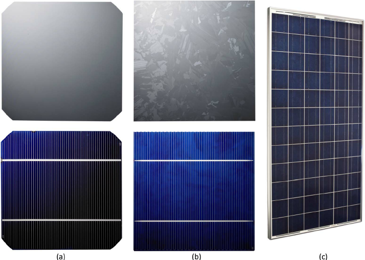
Two types of silicon wafers for solar cells: (a) 156-mm monocrystalline solar wafer and cell; (b) 156-mm multicrystalline solar wafer and cell; and (c) 280-W solar cell module (from multicrystalline wafers)
(Source: ResearchGate)
Cutting circular silicon wafers into polygons doesn’t change their electrical properties or utility as a semiconductor material.
In fact, this step is unnecessary in many applications — including most microchip manufacturing.
It’s entirely possible for solar cells to be circular.
However, you can fit more rectangular PV cells in a solar panel.
Polygonal-shaped wafers help simplify the manufacturing and assembly of PV modules comprised of multiple solar cells.
Cutting round silicon rods into polygonal shapes results in a significant amount of offcut, which is melted down and used to make polycrystalline solar cells.
That’s one reason why polycrystalline solar panels tend to be cheaper…
However, monocrystalline PV modules have much higher efficiency.
(Source: PV Manufacturing)
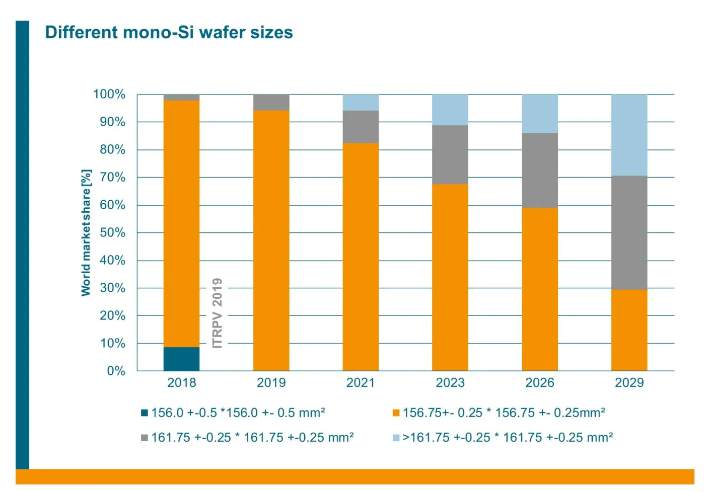
Monocrystalline Solar Wafer Sizes
Traditionally, the standard size for solar wafers has been 156mm2 — classed as MO.
In recent years, the diameter of silicon wafers manufacturers use for high-efficiency solar cells has increased — and so has the performance.
Wafers as large as 210mm2 (M12) are increasingly used in PV cells — a 35% increase in diameter from the original M0.
Much of the cost of manufacturing solar panels comes from the silicon wafer production process.
By increasing the size of the silicon wafers, manufacturers can produce photovoltaic cells that produce more rated power wattage without significantly raising costs over the long term — a win-win for factories and consumers.
Etching and Lapping
Both processes refine silicon wafers for semiconductor applications like solar cells and microchips.
Most solar-grade wafers are etched and lapped on each side.
Lapping is a mechanical process to smoothen a wafer’s surface and remove any silicon waste without causing damage.
A specialized pad and polishing liquid are typically used for lapping solar wafers.
Etching can be a chemical or physical process — or both.
The main goal of etching is to strip any remaining contaminants from the surface of the wafer.
Etching is also used to create antireflective layers on the wafers and improve the efficiency of solar cells.
Cleaning and Polishing
In the final stage of the production process, multiple steps are taken to ensure that the solar wafers are pristine and operate at the highest level of performance.
There are many methods of cleaning and polishing using chemical and mechanical processes.
The most common polishing method is chemical mechanical planarization (CMP), which produces a scratch and defect-free double-sided surface.
Photovoltaic Cell Manufacturing
Now that the production process is complete, boron-doped N-type and phosphorous-doped P-type wafers are combined to produce solar cells for use in panels and other modules like solar shingles.
Learn all about photovoltaic cell production here.
(Source: SEIA)
A Brief History of Solar Wafers
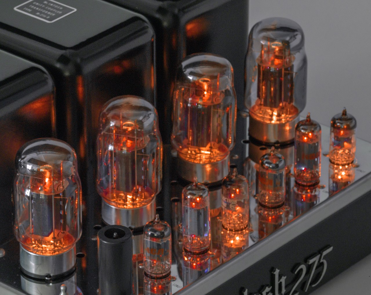
Before semiconductors became commercially viable, vacuum tube technology was used in many electronics.
With the advent of silicon and other semiconductors, vacuum tubes were relegated to specialized niches — like “vintage” guitar amps and high-end audiophile equipment.
(Source: Sebastian Nizan, CC BY-SA 4.0, via Wikimedia Commons)
.jpg)
Vacuum tubes are still used in many microwave ovens, but that’s in addition to solid-state semiconductor technology.
Here are some of the most common uses of semiconductors made from crystalline silicon wafers:
- Solar panels and other photovoltaic modules
- Integrated circuits (ICs) like microchips (computer chips), memory chips, and microprocessors
- Radio-frequency (RF) technology used in Internet of Things (IoT) and sensor technology
- Transistors
- Diodes
Chances are extraordinarily high that if you plug something into a wall socket, it will contain a silicon semiconductor.
But when were silicon wafers — like those used in most solar panels — first invented?
Here’s a timeline of milestone events.
- 1833: Michael Faraday discovers the semiconductor effect
- 1839: Edmond Becquerel discovers the photovoltaic effect
- 1884: Charles Fritts invents the first solar cell using selenium covered with a thin gold film
- 1940: Russel Ohl and Jack Scaff discover the p-n junction
- 1941: Russel Ohl patents the first silicon solar cell — it is 1% efficient
- 1950 – 1954: The diffusion process (doping) for silicon is developed at Bell Labs. By intentionally introducing impurities (boron and phosphorous) to silicon during the production process, solar cell efficiency dramatically improves
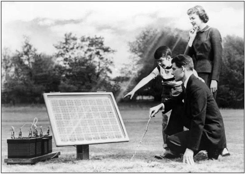
- 1954: Bell Labs announces the first solar panel. Calling it a ‘solar battery,” the device linked together several silicon solar cells with efficiency of about 6% The New York Times wrote that the breakthrough “may mark the beginning of a new era, leading eventually to the realization of one of mankind’s most cherished dreams–the harnessing of the almost limitless energy of the sun for the uses of civilization.”
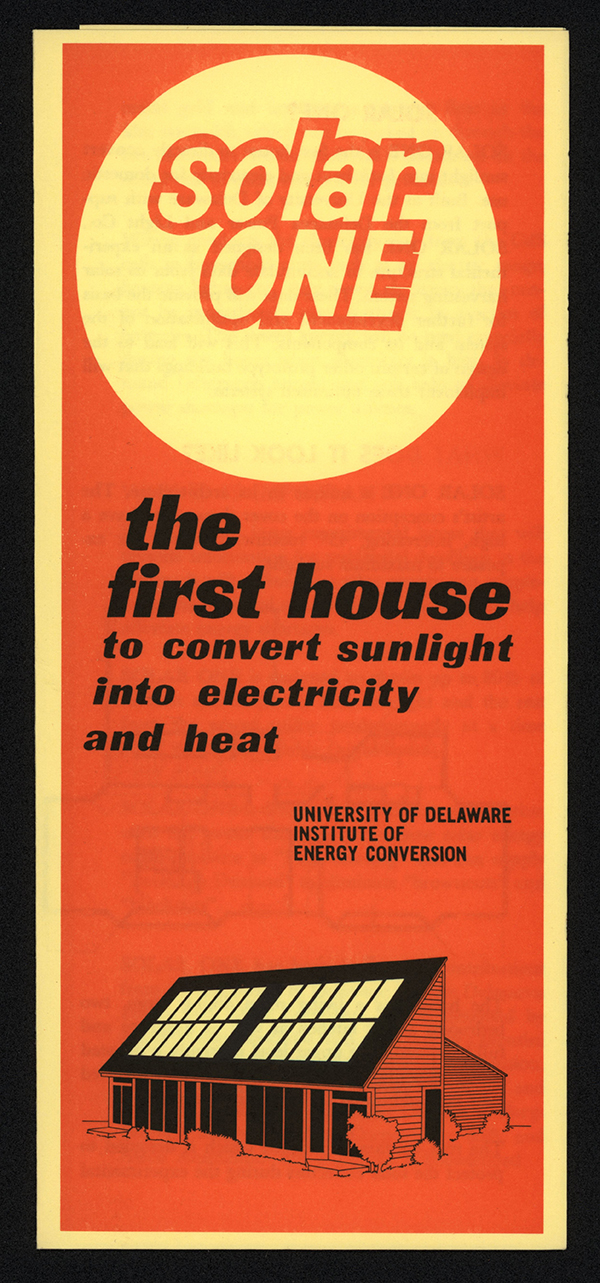
- 1973: Solar One is built at the University of Delaware. Billed as the “first solar house,” it relied on active and passive solar energy to supply electricity and heat.
- 1974: The Solar Energy Research, Development and Demonstration Act of 1974 is passed by US Congress during an energy crisis, marking the first big push from the government “to make solar viable and affordable and market it to the public.”
- 2006: The Solar Investment Tax Credit is enacted, incentivizing individuals to install solar panels and photovoltaics at home. It laid the foundation for the Residential Clean Energy Credit of 30% available to American taxpayers today.
(Source: SEIA)
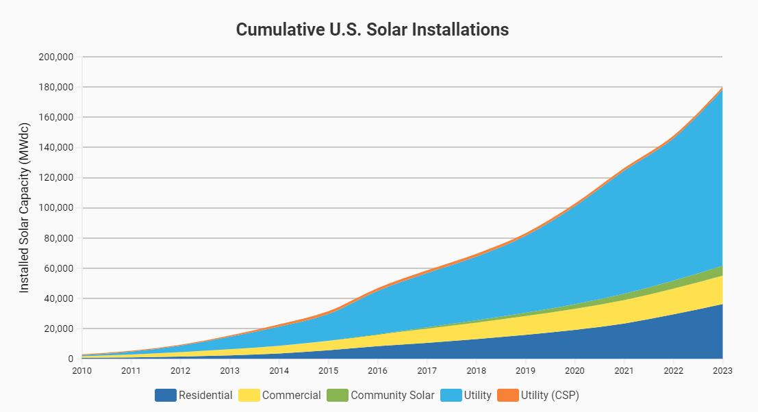
Since the mid-2000s, solar power adoption by industry and consumers has skyrocketed, growing by over 200x.
Silicon wafers have fueled the solar revolution since 1954, though the technology has come a long way since then!
Thanks to constant innovation, falling prices, and improvements in efficiency, silicon wafer-based solar cells are powering the urgent transition away from producing electricity by burning fossil fuels.
And will do for a long time to come.
What Are Thin Film Solar Cells?
Thin film solar cells are an alternative to wafer-based cells but provide much lower efficiency.
Thin film based solar panels are typically used under specific conditions in industrial-size photovoltaic applications.
The most common types of thin film solar cells and panels are:
- Amorphous silicon (a-Si)
- Cadmium telluride (CdTe)
- Copper indium gallium selenide or diselenide (CIGS)
- Perovskite
What Are the Advantages of Wafer-Based Solar Cells?
There are multiple reasons why wafer-based solar cells are the essential component in over 90% of photovoltaic panels and other modules sold worldwide.
Both polycrystalline and monocrystalline solar panels use wafer-based silicon solar cells.
The only alternatives to wafer-based solar cells that are commercially available are low-efficiency thin-film cells.
Higher Efficiency
Silicon wafer-based solar cells produce far more electricity from available sunlight than thin-film solar cells.
It’s helpful to note that efficiency has a specific meaning when applied to solar cells and panels.
It’s a spec that measures the wattage produced per square meter (m²) of photovoltaic material exposed to peak sunlight.
The average efficiency by solar cell type is as follows:
- Monocrystalline silicon wafer: 20% – 23%
- Polycrystalline silicon wafer: 15% – 18%
- Thin-film: 5% – 12%
Consequently, you would need far more surface area — and panels — to produce the same amount of electricity with thin film than with either mono or polycrystalline cells.
(Source: PV Magazine)
Falling Cost
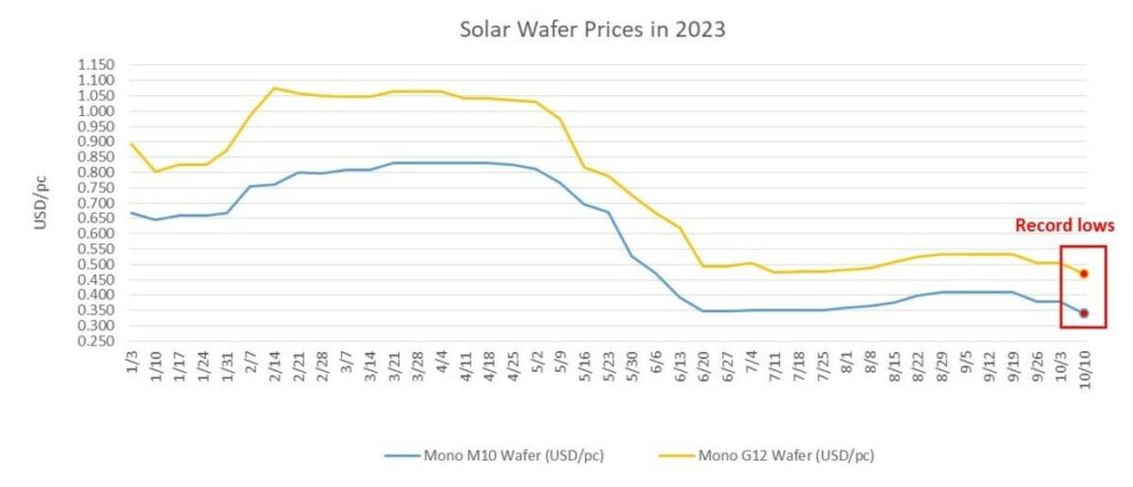
The price of solar-grade silicon wafers regularly hit record lows thanks to rising demand, improved technology, and economies of scale.
Government incentives — both to individuals and manufacturers — also contribute significantly to the falling cost and rising adoption of solar.
For example, the 30% Solar Tax Credit — officially known as the Residential Clean Energy Credit — can save US taxpayers 30% off the total purchase and installation costs of solar panels and the balance of system.
There are many state tax credits and other incentives to switch to solar, dramatically shortening the solar payback period and increasing return on investment.
Longevity and Durability
Polycrystalline and monocrystalline solar panels last for over 30 years on average and are designed to withstand extreme weather events.
Thin-film PV panels have a much shorter expected lifespan of 10 – 20 years.
Established Tech
Silicon wafer-based solar cells have long been the industry standard in photovoltaic applications worldwide.
That’s unlikely to change anytime soon.
Research and innovation are always ongoing but primarily focused on improving silicon wafer technology — not replacing it.
It’s also essential to remember that photovoltaic systems do not rely on solar panels alone.
Residential solar power systems are almost exclusively designed to be used with silicon wafer-based PV modules.
Frequently Asked Questions
Silicon wafers are by far the most widely used semiconductors in solar panels and other photovoltaic modules. P-type (positive) and N-type (negative) wafers are manufactured and combined in a solar cell to convert sunlight into electricity using the photovoltaic effect. Thin-film solar panels do not use wafers but are highly inefficient and only used in rare circumstances. Over 90% of solar panels use silicon wafers.
P-type (positive) and N-type (negative) silicon wafers are the essential semiconductor components of the photovoltaic cells that convert sunlight into electricity in over 90% of solar panels worldwide. Other solar cell components include printed silver paste and anti-reflective glass. Thin-film solar cells don’t use silicon wafers but are highly inefficient and rarely used.

Final Thoughts
Silicon wafer-based photovoltaic cells are the essential building blocks of modern solar technology.
EcoFlow’s rigid, flexible, and portable solar panels use the highest quality monocrystalline silicon solar cells, offering industry-leading efficiency for residential on-grid and off-grid applications.